Samsung Foundry has filed documents with authorities in Arizona, New York, and Texas seeking to build a leading-edge semiconductor manufacturing facility in the USA. The potential fab near Austin, Texas, is expected to cost over $17 billion and to create 1,800 jobs. If everything goes as planned, it will go online by the fourth quarter of 2023. There is an intrigue about the new fab though: Samsung hasn't stated which process node it will be designed for. Could Samsung be the first to 3nm in the USA?
Samsung Foundry to Expand in the USA
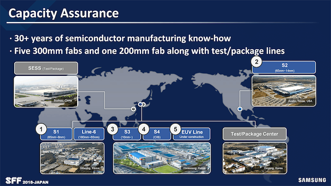
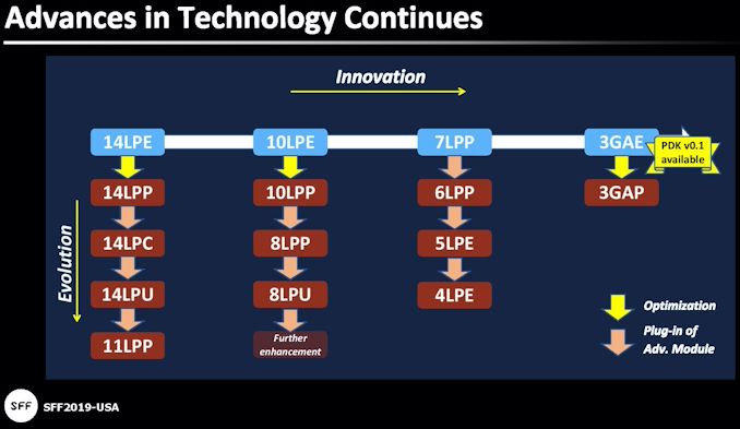
As demand for semiconductors is increasing, Samsung Foundry and other makers of chips are expanding their manufacturing capacities. In the recent years the company made chips using its leading-edge manufacturing technologies solely in South Korea, whereas its S2 manufacturing facility in Austin, Texas, was left with 14LPP (and derivatives down to 11LPP) and older fabrication processes that are too outdated for leading edge products. When it comes to chip design, Samsung has enough customers inside the US (such as IBM, Nvidia, Qualcomm, Tesla, just to name a few) that need to use its most advanced nodes and would prefer to use fabs located in the USA, which is why it needs to build a new manufacturing facility in this country. Furthermore, the company also needs a new leading-edge fab in North America to better compete against its rival TSMC, which plans to build a semiconductor production facility in Arizona by 2024.
Samsung Foundry officially began to explore possibilities to build a new fab in Arizona, New York, and Texas recently, according to Austin American-Statesman. The current plan submitted to the government of Texas includes a 7 million square feet (650 thousand square meters) facility on the company's 640-acre site (i.e., the fab will be adjacent to the existing S2) that will cost over $17 billion. The company has no plans to upgrade the S2 in the foreseeable future as mature process technologies are still required by its clients.
There are four criteria that the new location must meet in a bid to make sense for Samsung's leading-edge fab, according to the documents filed with the Texas authorities: access to talent, existing semiconductor manufacturing ecosystem, speed to market, and strong public- private partnership (i.e., incentives). Samsung already has a fab in Texas, so it already has talent and a supplier ecosystem in the state. By contrast, it will have to fight both for talent and supplies in Arizona (against Intel and TSMC) and New York (against GlobalFoundries).
To build a leading-edge manufacturing facility, Samsung needs rather huge incentives from authorities. In particular, Samsung is requesting combined tax abatements of $805.5 million over 20 years from Travis County and the city of Austin, according to Reuters, which essentially means that Samsung demands a 100% tax abatement from the county and 50% from the city. In addition, Samsung is seeking $252.9 million in tax breaks from the Manor school district based on the Texas Tax Code that allows property tax breaks for economic development projects. So far, no company has received a 100% tax abatement anywhere in the USA, according to market observers. Nonetheless, the deal still makes a lot of sense for the state, and there is likely going to be interest from the federal government as well.
"As there are other highly competitive markets seeking to win this expansion deal, it is imperative that our state and local governments work together to ensure Austin comes out on top," said Amber Gunst, CEO of the Austin Technology Council. "Not only does this provide 1,800 jobs that will be available to Central Texans of all education and skill levels, this expansion creates an even stronger relationship between Samsung and Austin, a relationship we value immensely."
Samsung expects the new fab to have an economic output of around $8.642 billion and salaries for permanent workers to total $7.323 billion in the first 20 years of its operation.
Project Silicon Silver: Coming Online in Q4 2023
The plans for the new fab are called Project Silicon Silver (PSS), and it will be located adjacent to S2. It will not use any of the existing buildings of S2, but will be a completely new fab constructed from the ground up. It will have its own operations support, central utility building, industrial waste treatment, air separation plans, storage for inert gases, and other constructions.
"The only currently-contemplated interconnections between the new facility and the surrounding existing property may be a pedestrian and/or material bridge or walkway constructed between the existing improvements on the site and the new construction," the document submitted to the authorities reads.
Samsung will spend $5.069 billion on buildings and real estate property improvements as well as $9.931 billion in semiconductor manufacturing equipment.
Samsung Foundry does not disclose many details about the new fab. At present, we know that if the company signs all necessary papers with the authorities in Austin, it will break ground by Q2 of 2021 with the expectation that production will be up and running by Q4 of 2023. In addition, we also know that the facility will occupy 650 thousand square meters of land. To put that number into context, TSMC's Fab 18 in Tainan (in the Southern Taiwan Science Park) will occupy 950 thousand square meters of land when it is fully built. In general, Samsung is planning to build a rather huge manufacturing facility. TSMC's Fab 18 has a goal of 120k-140k wafer starts per month at full volume, so we should expect PSS to be around the 70k-100k mark assuming identical requirements and scaling.
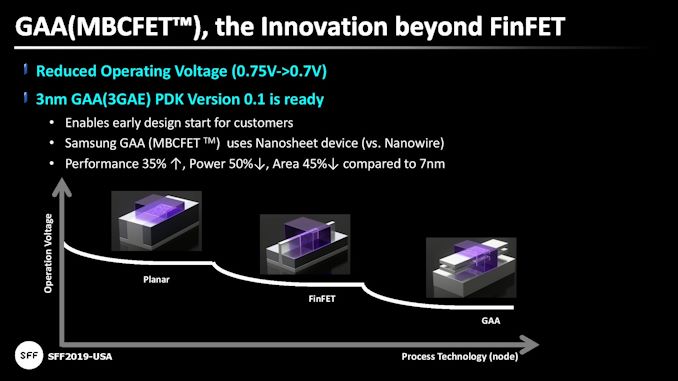
Samsung Foundry does not disclose which process technologies it plans to use at the new fab, but it is safe to say that they will use extreme ultraviolet (EUV) lithography. Considering the fact that Samsung expects its 3 nm technology based on gate-all-around (GAA) multi-bridge channel field effect transistors (MBCFETs) to be ready in 2021 ~ 2022 timeframe, it is logical to expect it to be used at the fab along with other technologies. In the end, Samsung's V1 fab in South Korea will be used for multiple nodes, including 3 nm.
Based on currently available information, Samsung is planning a bigger project than its rival TSMC. TSMC's planned fab in Arizona will have an initial production capacity target of about 20,000 wafer starts per month (WSPM) and will employ 1,600 people directly. TSMC intends to spend $12 billion on its new fab from 2021 to 2029, which indicates that TSMC's new fab will be a smaller facility when compared to the new Samsung fab in Texas.
No R&D Activities, Manufacturing Only
The documents that Samsung has submitted to the authorities clearly indicate that the Project Silicon Silver is a purely manufacturing facility and the company does not plan to run any R&D activities there.
Since there will be no research and development done at the new fab, Samsung Foundry will not be able to apply for any kind of USA government help when it comes to semiconductors R&D even after appropriate programs will be passed by the legislators.
Furthermore, Samsung's S2 fab does not have the USA Department of Defense's Trusted Foundry status, so it does not look like the company makes any chips for the DoD. In fact, it is unclear whether it is interested in military contracts in the USA in general.
Summary
After GlobalFoundries pulled out from developing leading-edge process technologies in 2018 and Intel lost its process technology lead to TSMC and Samsung Foundry, the USA government has been more willing to help local chipmakers in a bid to ensure that the country is self-reliant and does not depend on chips produced elsewhere.
TSMC was the first to take advantage of the USA willingness to assist local semiconductor production and its $12 billion fab in Arizona will start production of chips using its N5 node (and probably N5P and N4 derivatives) in 2024. Meanwhile, TSMC's fab in Arizona with an initial 20,000 WSPM capacity will not be as large as the facilities it has in Taiwan. To serve the USA government orders, TSMC's facility will have to gain the Trusted Foundry status, if/once it gets it, it will be able to sell authorities chips produced using a very advanced node. In addition to TSMC, some of its suppliers are also gearing up to build new facilities in the USA.
Samsung Foundry, the world's second largest contract maker of chips, is another foundry to build a leading-edge fab in the USA The company's Project Silicon Silver manufacturing facility in Texas will cost over $17 billion and is projected to be larger when compared to TSMC's fab in Arizona. It remains to be seen which process technology SF plans to use at the fab, but one of the options is its 3 nm MBCFET-based leading-edge node. Meanwhile, it is unclear whether Samsung is seeking to build chips for the USA government agencies.
While the USA government would prefer to help local chipmakers, such as Intel or GlobalFoundries, its initiatives to assist production of chips in the country have so far gathered significant interest from Taiwan-based TSMC and South Korea-based Samsung. In any case, it looks like the plan to bring leading-edge semiconductor manufacturing back to the USA works and a $27 million planned investment is a good proof of that, depending on tax abatements throughout the process.
Related Reading:
The Link LonkFebruary 10, 2021 at 11:30PM
https://ift.tt/2Z3Syc5
Samsung Foundry: New $17 Billion Fab in the USA by Late 2023 - AnandTech
https://ift.tt/2O3clnm
Samsung


No comments:
Post a Comment